I went into this assuming indium phosphide in data center optics was a recent development, something somebody figured out in the last couple of years as AI clusters got big. It isn’t. InP has been the standard laser material for fiber optics since the late 1970s, and it has been inside hyperscale data centers in volume since about 2016. What changed recently is how far the links have to reach, how fast they run, and how many network ports each accelerator needs. Each of those pushes more links onto single-mode fiber, and single-mode fiber at these wavelengths means an InP laser.
Why InP
Silica fiber has its lowest loss in two wavelength windows, around 1.3 and 1.55 microns. In 1979 an NTT group led by T. Miya measured 0.2 dB/km at 1.55 microns, which is close to the theoretical floor for silica glass. To use those windows you need a semiconductor whose bandgap emits there and whose crystal lattice can be grown cleanly. Indium gallium arsenide phosphide alloys grown on an InP substrate are that material. J.J. Hsieh at MIT Lincoln Laboratory made the first InGaAsP/InP lasers in 1976 and got them to 1.3 microns in 1977. Bell Labs, NTT, and the Japanese component makers had products within a few years. Every long-haul, metro, and undersea fiber link since then has used InP lasers and InP-family photodetectors.
So the question of who discovered that InP works in optical interconnects has a boring answer: a few lab groups between 1976 and 1980. The telecom industry has been running on it for over forty years.
Why data centers came to it later
Data centers didn’t need it for a long time. Links inside a building were short, and the cheapest way to move data a hundred meters over fiber is a gallium arsenide VCSEL at 850 nm on multimode fiber. That is what Gigabit Ethernet and Fibre Channel used from the late 1990s, and it is still on a lot of server ports today. Multimode fiber is cheap, the lasers are cheap, and the alignment tolerances are loose. If the longest link in the building is a hundred meters, there is no reason to pay for InP.
What I hadn’t appreciated is how directly the link distances inside a facility drive the choice of optics. The reach a transceiver has to cover is a design input, and it comes out of the floor plan.
Reach gets shorter as speed goes up
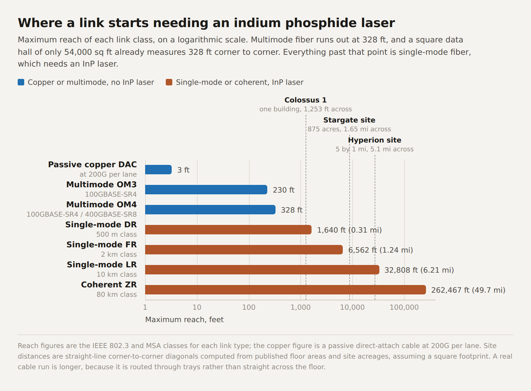
Multimode fiber is limited by modal dispersion, and the usable reach roughly halves each time the data rate doubles. A 10G link runs 400 meters on OM4 multimode. A 100G-SR4 link runs 100 meters on the same fiber, which is 328 feet. 400G-SR8 is also 100 meters and needs OM4 to get there. Copper is worse. A passive direct-attach cable that could carry 5G for three meters carries 200G per lane for about one meter. So every step up in speed moves some links from copper to fiber and some links from multimode to single-mode, and the single-mode links need InP lasers.
The building was already too big for multimode
Meta wrote this down in 2017 when it explained its 100G design. At 40G its data centers were cabled with OM3 multimode fiber. Getting 100 meters at 100G on the same layout would have meant recabling with OM4, and Meta’s own assessment was that this “does not allow any flexibility for longer link lengths or for a data rate evolution beyond 100G.” So it moved to single-mode fiber for everything. It took the CWDM4 spec, cut the reach requirement from 2 km to 500 meters, narrowed the operating temperature range to 15 to 55 °C, and lowered the link budget from 5 dB to 3.5 dB, on the reasoning that a data center is a controlled environment and the spec could be written to match it. The cost argument was that fewer fibers and patch panels more than paid for the more expensive single-mode transceivers. Microsoft reached a similar answer by a different route and standardized on PSM4, four parallel single-mode fibers with a minimum reach of 500 meters. Both of those module types use four InP DFB lasers each, and they were deployed by the hundreds of thousands from 2016 on.
The 500 meter figure is the useful number here, and it is not a guess. It is what two operators independently concluded their in-building links had to cover. A hundred meters of multimode does not cross a hall of a few hundred thousand square feet, particularly once the cable is routed through trays rather than running in a straight line. Hyperscale buildings have been that size since well before AI, so the move to single-mode was settled on ordinary data centers in 2014 to 2016 and was not caused by AI at all.
The AI sites are not really an exception to that. Colossus 1 in Memphis is a converted 785,000 square foot plant, and Apple’s data center in Mesa, which has nothing to do with AI training, is a single building of 1.3 million square feet. What separates an AI facility from a conventional one is power, not floor area. Current AI builds run somewhere between 100 and 750 MW per site, and a rack of accelerators draws 50 kW or more against 8 to 12 kW for a rack of conventional servers. When Colossus gets described as the largest thing of its kind, which it is, the claim is about GPU count and power rather than the size of the building: roughly 555,000 GPUs and about 2 GW as of February.
Power is what matters for the optics, in two ways. Power density is what fills a hall with accelerators, and each accelerator brings its own network ports. And because the power available at any one site is capped by the grid and by what can be cooled, large training capacity gets built as several buildings wired together rather than as one enormous hall. Stargate’s Abilene site is eight buildings of roughly 485,000 square feet each across 875 acres. Meta’s Hyperion site in Louisiana has been described as five miles by one mile. Links between buildings on a site like that are past what 500 meter and 2 km optics cover, so they move to 10 km LR and to coherent optics, which are also built on InP.
More ports per accelerator
A traditional data center server had one or two 10G or 25G network ports. In an AI cluster, every GPU gets its own 400G or 800G NIC for the back-end network, and every one of those ports has a transceiver in it, plus the switch tiers above. NVIDIA’s own example at GTC 2025, for a cluster of over 100,000 GPUs in a full fat-tree topology, came to 2.4 million optical transceivers. That is the order-of-magnitude change Lumentum’s CEO was describing when he said telecom customers used to buy lasers by the hundreds and the hyperscalers now want hundreds of millions.
Silicon photonics does not change this. Intel’s 2016 silicon photonics 100G PSM4 module still had InP laser die bonded onto the silicon, because silicon cannot lase. Co-packaged optics, which NVIDIA announced at GTC in March 2025 and began shipping in switches this year, moves the modulator and waveguide onto silicon and moves the lasers to an external source module. The lasers in that module are InP. CPO reduces the number of lasers per port. It does not reduce the number of ports.
How much building is actually going on
Most of the demand numbers in this area come from the people selling the parts, so it is worth checking the build-out against something neither a vendor nor an analyst controls. The Census Bureau publishes monthly value-of-construction-put-in-place figures, and since 2014 the private series has carried a line item called “Data center.” It is a free public-domain workbook, it runs about two months behind, and it is as close to a count of concrete being poured as this sector has.
Annual private data center construction, in nominal dollars:
| Year | Spend |
|---|---|
| 2019 | $8.5B |
| 2022 | $12.6B |
| 2023 | $20.0B |
| 2024 | $34.8B |
| 2025 | $49.7B |
| July 2026 | $6.6B in the month, about $79B annualized |
The July 2026 figure is up 58% on the same month a year earlier, so the rate is still climbing rather than flattening. Every one of those buildings gets cabled, and at current lane rates most of that cabling terminates in a single-mode transceiver.
The same workbook carries a useful contrast. Construction of computer, electronic and electrical manufacturing plants, which is where the CHIPS Act fab boom shows up, peaked in 2024 at about $122B and was down 47% year over year in July 2026. The fabs were built first. The data centers that fill them with orders are being built now, and the optics demand tracks the second line rather than the first.
What changed in 2025 and 2026
Two things, and neither is a discovery.
The first is that the transmitter mix moved toward the part of the market where InP has the least competition. At 25G and 50G per lane a directly modulated laser was good enough. At 100G and now 200G per lane, the preferred transmitter for anything beyond a few hundred meters is an electroabsorption modulated laser, which is an InP DFB laser with an InP modulator grown on the same chip. The 800G and 1.6T modules that AI clusters are buying are built around these.
The second is supply. China added indium phosphide and trimethylindium to its dual-use export control list on February 4, 2025. China refines roughly 70% of the world’s indium. AXT’s substrate business is in Beijing and has been shipping under per-customer export permits since then. Lumentum’s CEO said this summer that the company was shipping more than 30% below what customers wanted, across five InP fabs. In March NVIDIA invested $2 billion in each of Lumentum and Coherent, with purchase commitments and capacity rights attached. On the substrate side, Coherent moved its Sherman, Texas fab to 6-inch InP wafers, which it says gives 4x the capacity and a 60% reduction in die cost, and in June signed AXT to a three-year supply agreement for 6-inch substrates with a prepayment.
So the material was already in every hyperscale data center for a decade. Then the buildings got large enough that most links needed single-mode optics, the lane rates went high enough that those links needed EMLs, the port count per accelerator went up by an order of magnitude, and the main source of the raw material went under export licensing. That combination is what made a fifty-year-old technology look like a new one.
What I still want to check
- When 40G LR4 and 100G LR4 first shipped into hyperscale in volume. That would probably move the start date for InP in the data center back to around 2010.
- Whether 200G-per-lane transmitters are really as InP-dominated as the supplier presentations suggest, or whether silicon photonics with external InP lasers takes a meaningful share of 1.6T.
- What fraction of links in a Colossus- or Stargate-class site are actually FR or LR class rather than DR, and how many cross between buildings rather than staying inside one. That would say how much of the InP demand comes from the campus layout and how much from the port count.
- Data hall square footage rather than gross building footprint for the AI sites, since white space is usually only 40 to 50% of the gross area and the published figures are almost all gross.
- How much of the price move in InP substrates is export licensing and how much is real limits on crystal growth capacity.
- Whether InP substrate and laser trade shows up cleanly in UN Comtrade or the Census trade API under a specific commodity code. If it does, import volumes would be a way to watch the export controls bite without relying on any supplier’s commentary.